C16MX750
Universal Asynchronous Receiver/Transmitter with FIFOs
Function Description
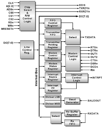
The C16MX750 programmable asynchronous communications interface (UART) core provides data formatting and control to a serial communication channel.
The core has select, read/write, interrupt and bus interface logic features that allow data transfers over an 8-bit bi-directional parallel data bus system. With proper formatting and error checking, the core can transmit and receive serial data, supporting asynchronous operation.
Features
- Capable of running with all existing 16450 and 16550A Software
- Standard Asynchronous Communication Bits (Start, Stop, and Parity) Added or
Deleted to or From the Serial Data Stream
- In FIFO mode, Transmitter and Receiver are each buffered with Programmable 16- or 64-Byte FIFOs to Reduce CPU Interrupts
- Programmable Auto- RTS\ and Auto- CTS\
- In Auto- CTS\ Mode, CTS\ Controls Transmitter
- In Auto- RTS\ Mode, Receiver FIFO Contents and Threshold Control RTS\
- Serial Ports Have Infrared Data Association (IrDA) Inputs and Outputs
(OPTIONAL)
- Fully Programmable Serial Interface Characteristics:
- 5-, 6-, 7-, or 8-Bit Characters
- Even-, Odd-, or No-Parity Bit Generation and Detection
- 1-, or 2-Stop Bit Generation
- Baud Generation (DC to Silicon dependent Mbits Per Second)
- Parity, overrun and framing error checking
- Supports up to 15 Mbps transmission rates
- (Typical value: silicon dependent)
- Programmable Baud Rate Generator allows division of any reference clock by 1
to (216-1) and generates an internal 16 X Clock
- False start bit detection
- Automatic break generation and detection
- Break, Parity, Overrun, Framing Error Simulation
Peripheral modem control functions
- The C16MX750 was developed in VHDL/Verilog HDL and synthesizes to
approximately 6,500 gates depending on the process used
- After Reset, All Registers Are Identical to the TL16C450 Register Set
- In the TL16C450 Mode, Hold and Shift Registers Eliminate the Need for Precise
Synchronization Between the CPU and Serial Data
- Independent Receiver Clock Input
- Independently Controlled Transmit, Receive, Line Status, and Data Set
Interrupts
- Complete Status Reporting Capabilities
- Internal Diagnostic Capabilities:
- Loopback Controls for Communications Link Fault Isolation
- Break, Parity, Overrun, Framing Error Simulation
- Modem Control Functions ( CTS\, RTS\, DSR\, DTR\, RI\, and DCD\)
- Fully Prioritized Interrupt System Controls
Symbol
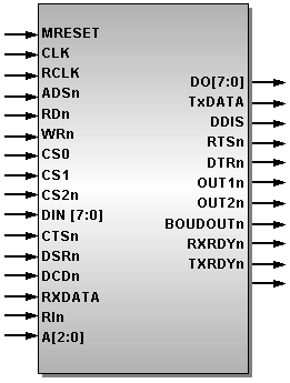
Pin Description
| Name | Type | Polarity | Description |
| RESET | In | High | External Reset |
| CLK | In | - | Master Clock |
| RCLK | In | - | Receive Clock |
| ADSn | In | Low | Address Strobe |
| RDn | In | Low | Read Control |
| WRn | In | Low | Write Control |
| CS0 | In | High | Chip Select 0 |
| CS1 | In | High | Chip Select 1 |
| CS2n | In | Low | Chip Select 2 |
| DIN[7:0] | In | - | Data Input Bus |
| CTSn | In | Low | Clear-to-Send |
| DSRn | In | Low | Data Set Ready |
| DCDn | In | Low | Data Carrier Detect |
| RXDATA | In | - | Receive Data |
| RIn | In | Low | Ring Indicator |
| A[2:0] | In | - | Register Select |
| D0[7:0] | Out | - | Data Output Bus |
| TXDATA | Out | - | Transmit Data |
| DDIS | Out | High | Driver Disable |
| RTSn | Out | Low | Request-to-Send |
| DTRn | Out | Low | Data Terminal Ready |
| OUT1n | Out | Low | Output 1 |
| OUT1n | Out | Low | Output 2 |
| TxRDYn | Out | Low | Transmit Ready |
| RxRDYn | Out | Low | Receiver Ready |
| INTRPT | Out | High | Interrupt |
| BOUDOUTn | Out | Low | Baud Out |