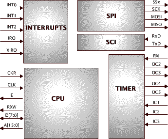
C68MX11 CPU Core
General Description
The
C68MX11 CPU core is based on the Motorola M68HC11 microcontroller controller, but has an
enhanced full 16 bit architecture, thus requiring less clock cycles for completing a large
number of instructions compared with the original device. In addition to executing all
M6800 and M6801 instructions, the C68MX11 instruction set includes more than 90 new
opcodes as in the original M68HC11.
A
large number of peripheral modules can be added to achieve highly sophisticated, on-chip
capabilities, as for example a complete 16 bit timer system with 3 input capture lines, 5
output compare lines and real-time interrupt function, and an asynchronous or synchronous
serial communication interface. Pins for complete monitoring of internal registers have
been added for test purpose.
Features
¨ Enhanced
16 bit architecture
¨ Machine
Software
compatible with industry standard M68HC11
¨ Byte
efficient instructions, powerful addressing modes, 8x8 multiplication supported
¨ Less
machine-cycles per operation
¨ Memory
mapped I/O
¨ Parallel
I/O system
¨ Real
time interrupt system (RTI)
¨ Synchronous
Serial Peripheral Interface system (SPI)
¨ Full-duplex
UART system (SCI)
¨ 16
bits timer system includes 3 input capture and 5 output compare systems
¨ 8
bits pulse accumulator
¨ Watchdog
system (COP) interrupt available
¨ Clock
monitor fail interrupt available
¨ Address
space of 64 KBytes
¨ No
internal reset generator or gated clock
¨ SYNCHRONOUS
RESET ; the
C68MX11 has 3 reset vectors sources, which easy identify a cause of system reset.
¨ Fully
synthesizable, static synchronous design with no internal tri-states
¨ VHDL
Test bench provided
¨ De-multiplexed
Address/Data Bus to allow easy connection to memory available
on request
Symbol
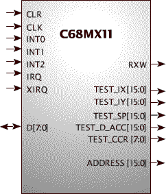
Pin Description
Name |
Type |
Polarity |
Description |
RESETN |
In |
Low |
External Reset |
CLK |
In |
- |
Master
Clock |
E |
Out |
- |
Master
Clock E |
AS |
Out |
High |
Address
Strobe |
RXW |
Out |
- |
Read/Write
Control |
CMIRQN |
In |
Low |
Clock
Monitor Interrupt |
COPIRQN |
In |
Low |
COP
Interrupt |
COP_EN_N |
In |
Low |
COP
Interrupt Enable |
XIRQN |
In |
Low |
External
Interrupt |
IRQN |
In |
Low/Edge |
Non-maskable
Interrupt |
PE_IN[7:0] |
In |
- |
Port E Input |
PC_DATA_IN[7:0] |
In |
- |
Port C Input
(I/O) |
PC_DATA_OUT[7:0] |
Out |
- |
Port
C Output (I/O) |
PC_DDR[7:0] |
Out |
- |
Port
C data direction (I/O) |
PB_OUT[7:0] |
Out |
- |
Port B Output
(I/O) |
PA20[2:0] |
In |
- |
Port
A Input (I/O) Bit 2 to 0 |
PA63[6:3] |
Out |
- |
Port
A Output (I/O) Bit 6 to 3 |
PA7 |
In |
- |
Port A Input
(I/O) Bit 7 |
DDRA |
Out |
- |
Port
A bit 7 tri-state buffer enable |
PORT_A7_OUT |
Out |
- |
Port
A Output (I/O) Bit 7 |
DDRD[5:0] |
Out |
- |
Port
D data direction (I/O) |
PORTD_OUT[5:0] |
Out |
- |
Port
D Output (I/O) |
PD[5:0] |
In |
- |
Port
D Input (I/O) |
PC_IN[7:0] |
In |
- |
Port
C Input (Multiplexed address/data) |
PC_OUT[7:0] |
Out |
- |
Port
C Output (Multiplexed address/data) |
PC_EN |
Out |
- |
Port
C tri-state buffers enable |
PB[7:0] |
Out |
- |
Port
B Output (address [15:8]) |
TXDATA |
Out |
- |
SCI
transmit data |
MISOO |
Out |
- |
SPI
Master In Slave Out Output |
MOSIO |
Out |
- |
SPI
Master Out Slave In Output |
SCKO |
Out |
- |
SPI
Clock Output |
RXW |
Out |
- |
Read/Write
Control |
TEST_IX[15:0] |
Out |
- |
Test
Index Register IX (test purpose only) |
TEST_IY[15:0] |
Out |
- |
Test
Index Register IY (test purpose only) |
TEST_SP[15:0] |
Out |
- |
Test
Stack Pointer SP (test purpose only) |
TEST_D_ACC[15:0] |
Out |
- |
Test
Accumulator D (test purpose only) |
TEST_CCR[7:0] |
Out |
- |
Test
CCR Register (test purpose only) |
DATA[7:0] |
Out |
- |
Data
Bus (demultiplexed) |
ADDRESS[15:0] |
Out |
- |
Address
Bus (demultiplexed) |
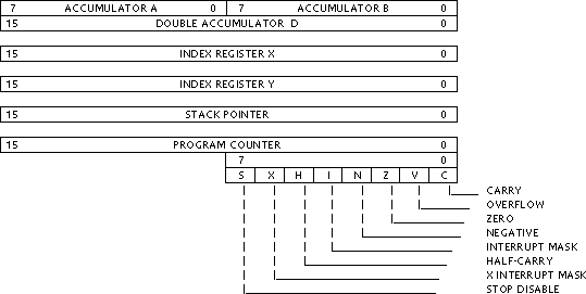
Programmer's Model
Block Diagrams
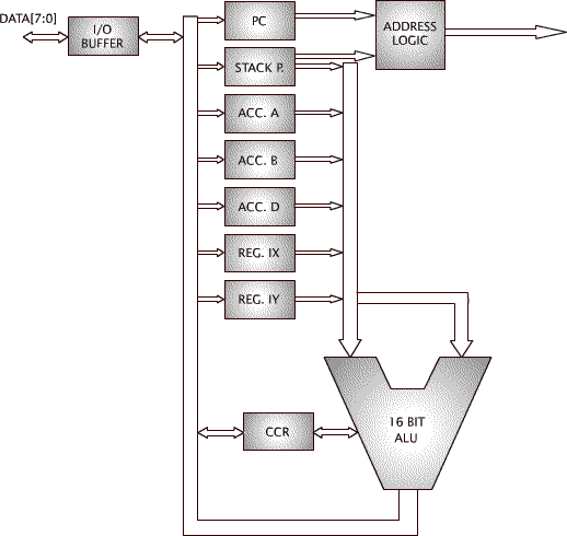
CPU
C68MX11 CPU Core
Functional Description
The central processing unit (CPU) of the 68MX11 has more
than 300 instruction opcodes and 6 addressing modes can be used to reference memory:
· IMM - immediate (the actual
argument is contained in the byte(s) immediately following the instruction)
· DIR - direct (the least
significant byte of the effective address of the instruction is contained in the byte
following the opcode. The high-order byte of the effective address is assumed to be 00
hex)
· EXT - extended (the
effective address explicitly appears in the 2 bytes following the opcode)
· IND - indexed (either index
register IX or IY is used for effective address calculation)
· INH - inherent (the operands
are CPU registers and they are inherently known by the CPU)
· REL - relative (used only
for branch instructions)
The CPU is able of addressing 64 Kbytes of memory. I/O
access is memory-mapped. Although the data busses have a width of 8 bit most of the
instructions have 16 bit equivalent instructions. The C68MX11 offers multiply, add,
subtract, compare, increment & decrement, load & store, and shift instructions of
16 bit operands. The CPU consists of two general-purpose 8-bit accumulators
used to hold operands and results of arithmetic calculations or data manipulations. The
accumulator A and B can be combined into a 16 bit double accumulator D. The 16 bit index
registers IX and IY are used for indexed addressing modes. The CPU automatically
supports a program stack. This stack may be located anywhere in the 64 Kbyte address space
through the stack pointer and may be any size up to the amount of memory
available in the system. The condition code register (CCR) contains five
status indicators (carry, overflow, zero, negative, and the half carry flag), two
interrupt masking bits (IRQ and XIRQ mask), and a STOP disable bit.
Core Assumptions
The design is fully synchronous and
doesn’t contain any internal tristate buses, therefore special considerations for
synthesis can be avoided. The design offers all of the original 308 opcodes and behaves
exactly in the same manner as the original 68HC11,with the exception discussed below. Due
to this modification the C68MX11 has actually 301 Opcodes
The variation from the original device are as following:
· The following OPCODES and relative mnemonics
have been NOT implemented in order to save area or because they would have made no sense
in the core implementation (TEST). If required they can be implemented on request.
1. FDIV INH Opcode 03
2. IDIV INH Opcode 02
3. STOP INH Opcode CF
4. TEST INH Opcode 00
The C68MX11 core is licensed from
Moxsyn S.r.l.
All trademarks mentioned in this document are trademarks of their respective owners.
Please send your
comments to webmaster@moxsyn.com