C68MX03
MPU Core
Function Description
The C68MX03 MPU core is based on the Motorola M6803U4
microcontroller. In addition to executing all M6800 and M6801 instructions, the C68MX03
instruction set includes 16 new opcodes as in the original MC6803U4.
On-chip resources include 192 bytes of RAM, a serial communications interface (SCI),
parallel I/O and 16-bit six-function timer. A large number of peripheral modules can be
added to achieve highly sophisticated, on-chip capabilities, as for example a complete
other 16 bit timer submodules and asynchronous or synchronous serial communication
interfaces.
Features
- 8 bit architecture
- Machine code 100% compatible with MC6803U4
- Byte efficient instructions, powerful addressing modes, 8x8 multiplication supported
- Fully static logic implementation - clock frequencies from DC to MHz
- Memory mapped I/O
- Interrupt logic same as the M6803U4
- Default memory organization compatible with M6803U4 systems
- Address space of 64 KBytes
- Bus compatibility with M6800 family
- Serial Communication Interface (SCI)
- 16-Bit Six Function Programmable Timer
- 2 Input Capture Functions / 3 Output Compare Functions
- 192 Bytes of RAM
- 29 Parallel I/O
- Fully synchronous VHDL 1076-93 design
Symbol
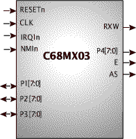
Pin Description
| Name |
Type |
Polarity |
Description |
| RESETn |
In |
Low |
External Reset |
| CLK |
In |
- |
Master Clock |
| IRQ1n |
In |
Low |
External Interrupt |
| NMIn |
In |
Low |
Non-maskable Interrupt |
| P1[7:0] |
Inout |
- |
Multifunction pis |
| P2[7:0] |
Inout |
- |
Multifunction pis |
| P3[7:0] |
Inout |
- |
Multifunction pis |
| RXW |
Out |
Low |
Read Write Control |
| AS |
Out |
Low |
Address Strobe |
| P4[7:0] |
Out |
- |
Multifunction pis |
| E |
Out |
- |
Output Clock |
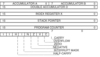
Programmer's Model
Block Diagrams
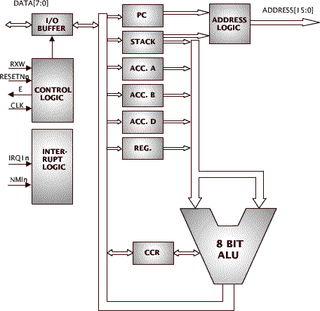
MPU
C68MX03 Microcontroller
Functional Description
The central processing unit (MPU) of the C68MX03 has more than 300 instruction opcodes
and 6 addressing modes that can be used to reference memory:
- IMM - immediate (the actual argument is contained in the byte(s)
immediately following the instruction)
- DIR - direct (the least significant byte of the effective address of
the instruction is contained in the byte following the opcode. The high-order byte of the
effective address is assumed to be hex 00)
- EXT - extended (the effective address explicitly appears in the 2 bytes
following the opcode)
- IND - indexed (either index register IX or IY is used for effective
address calculation)
- INH - inherent (the operands are CPU registers and they are inherently
known by the CPU)
- REL - relative (used only for branch instructions)
The CPU is able of addressing 64 KBytes of memory. I/O access is memory-mapped.
Although the data busses have a width of 8 bit, most instructions have a 16 bit equivalent
instruction. The C68MX03 offers multiply, add, subtract, compare, increment &
decrement, load & store, and shift instructions of 16 bit operands. The CPU consists
of two general-purpose 8 bit accumulators used to hold operands and
results of arithmetic calculations or data manipulations. The accumulator A and B can be
combined into a 16 bit double accumulator D. The 16 bit index registers
IX is used for indexed addressing modes. The CPU automatically supports a program stack.
This stack may be located anywhere in the 64 KByte address space through the stack
pointer and may be of any size up to the amount of memory available in the
system. The condition code register (CCR) contains five status indicators
(carry, overflow, zero, negative, and the half carry flag.
Core Assumptions
The design is fully-synchronous, and doesn’t contain any internal
tristate buses, therefore special considerations for synthesis can be avoided. The design
offers all of the original 321 opcodes and behaves exactly in the same manner as the
original M6803, with the exceptions discussed below.
The variations from original device are as following:
- Analog functionality is not be modeled such as the RAM control register bit (RAME) which
indicates when VCC has dropped under a certain value.
- The MC6803 has 2 mode of operations. The modes are chosen by the value of 3 lines during
the rising edge of reset. To make the core synchronous these 3 lines are latched on the
first clock edge after reset.
- Inside the SCI (UART) sub-module the Biphase Format has not been modeled.
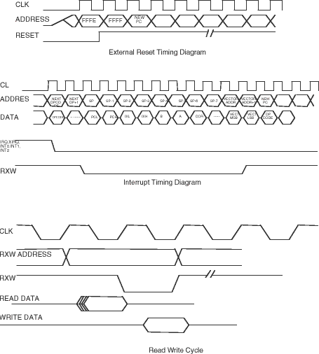
Timing Diagrams
Verification Methods
The C68MX03 MPU core’s functionality was verified by means of a
proprietary hardware modeler. The same stimulus was applied to a hardware model which
contained the original Motorola 6803U4 chip, and the results compared with the core’s
simulation outputs.
Related Information
Motorola Microprocessor data 1984 Data Book
Contact: Motorola Semiconductors, The Literature Distribution Center, http://mot-sps.com/
Deliverables
Gate-level Licenses
- Post-synthesis gate-level netlist
- Testbench
- Vectors for testing the functionality of the core
- Expected results for testbench
VHDL Source Licenses
- VHDL RTL source code
- Testbench
- Vectors for testbench
- Simulation script
- Synthesis script
- Expected results for testbench
All trademarks mentioned in this document are trademarks of their respective owners.
Please send your comments to webmaster@moxsyn.com